Applicants
for India's $10 Billion Incentive Scheme for Semiconductors
[ABS
News Service/25.02.2022]
On 15th Dec 2021, the government of
India had announced a new incentive scheme worth Rs.76,000 crore INR (nearly
$10.2 billion) in a bid to boost the semiconductor ecosystem in the country.
The policy broadly aimed at supporting
4 "buckets" of initiatives summarised as
below.
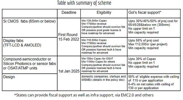
Rs 76,000 crore Semiconductor Mission
The Union Government on Saturday (Feb
19) announced the
details of the companies and consortiums that have applied in each of these
incentive 'buckets', and in some cases the quantum of total investment planned
and the total incentives sought from the government.
Here is what we know about the firms
and consortium that have applied for semiconductor incentive scheme.
1.
Category-A: Silicon (CMOS) fabs
Vedanta Foxconn JV, IGSS Ventures, and
ISMC have proposed to set up electronic chip manufacturing plants with
investments totaling $13.6 billion and have sought the support of $5.6 billion
from the Centre under the Rs 76,000 crore Semicon India Programme.
The applications have been received
for setting up 28 nm to 65nm Semiconductor Fabs with
a capacity of approx. 120,000 wafers per month.
A) ISMC is the proposal by Abu
Dhabi-based Next Orbit Ventures, representing a consortium of investors, for
establishing a semiconductor fab factory in India
The consortium is likely to have
submitted an application for the Analog Fab in technology partnership with
Israel-based Tower semiconductors (which is now in the process of being acquired
by Intel Foundry Services).
In an exclusive interview with Swarajya
in July 2021, Ajay Jalan, the founder and managing director of Next Orbit
Ventures, spoke
extensively on his ambition to establish a semiconductor fab factory in India.
ISMC proposes to establish a fab at
the cost of a $3 billion project and if selected, it is eligible for an
incentive from center up to $0.9 billion. The likely location is Dholera SIR in Gujarat.

ISMC
Proposal
B) Vedanta in JV with Foxconn has reportedly
submitted a $7.4 billion proposal for setting up a 28nm fab. The company is
venturing in to in a chip manufacturing unit in partnership with Hon Hai
Technology Group (Foxconn),
If the project proposal is approved,
Vedanta-Foxconn JV will qualify for up to $3.7 billion from the Union
Government
The company said that it expects the
fab unit to become operational by 2024. It is in process of looking at a
suitable location for the fab.
"Foxconn, though with no prior
manufacturing experience in semiconductors, was the perfect partner for the
project given its global footprint in electronics manufacturing" ET
quoted, Akarsh Hebbar,
global managing director of Vedanta Group’s display and semiconductor business,
as saying.
Foxconn is likely to invest around
$118 -$120 million as part of a joint venture.
C) IGSS Ventures Pte
Ltd (IGSSV). IGSS Ventures is a technology investment holding company that focuses on "building
companies with competitive advantages in ground-breaking technologies".
Very few details are available on the proposal or technology partnership it has
forged.
If one were to do a
back-of-the-envelope calculation based on the incentives offered by the
government, the IGSS proposal maybe for $3.2 billion with an incentive sought
likely to be tune of close to $1 billion. The investment size means that IGSS
is likely to have proposed setting up a 65nm (or close) fab.
2.
Category-B: Display fabs
Two companies, Vedanta and Elest, have proposed to set up a display manufacturing unit
with a projected investment of USD 6.7 billion and have sought the support of
USD 2.7 billion from the Centre under the Scheme for setting up of Display Fabs in India.
Setting up display fabs
has been identified as a priority area by the government. Display units account
for up to 25% of the Bill of Materials (BoM) for smartphones and 50% for TVs.
Despite huge growth in overall electronic exports, significant value addition
potential is lost due to the lack of display fab capabilities within the
country
Elest Private Limited lists Rajesh Mehta
and Prashant Mehta as directors. The duo founded Rajesh Exports, an Indian multinational gold
retailer headquartered in Bangalore, Karnataka. The group refines, designs, and
sells gold and jewelry. It is one of India's biggest exporters with plants that
have a processing capacity of 250 tonnes of jewelry
and gold products per annum.
Detailed information is not available
on the technology partnership for Vedanta's display fab foray. The company has
said that it plans to $10 billion on displays.
Though the policy gives up to 50%
incentive for approved display fabs, there is a
ceiling of INR 24000 crore (approx $1.6 billion) per
project. It is likely that one of the applicants may have proposed a $4.5
billion display fab project for a $1.6 billion incentive, while the other
applicant would have proposed to set up a $2.2 billion project for a $1.1
billion incentive.
The government's press release noted
that the first round of applications was invited till 15.02.222 which hints at
the possibility of inviting applicants in the future also.
For the next two categories - Compound
semiconductors-OSAT and design companies, the government while unveiling the
policy had announced the application deadline as 1 Jan 2025. However it
information on applications received so far. These categories continue to be
open for applications and we are likely to see more names in future.
3.
Category-C: Compound semiconductors and OSAT
Four companies - SPEL Semiconductor
Ltd., HCL, Syrma Technology, and Valenkani
Electronics, have applied for incentives under the scheme for semiconductor
Packaging. Ruttonsha International Rectifier Ltd. has
registered under this Scheme for Compound Semiconductors.
The only name that has come out so far
for compound semiconductors - Ruttonsha - had been in
the news
being in association with Visicon power
The company founder Harshad Mehta has said that the process of setting up a
semiconductor fab in Baroda. "Our plan right now is to transfer the
technology from our Oregon fab to the one in Baroda" he noted.
SPEL Semiconductor: The company website claims "Being India’s first
& only Semiconductor IC Assembly & Test facility, SPEL pioneered the
Indian OSAT market". It is not known yet if the proposal is to expand
their existing facility in Chennai or a fresh new factory
HCL technologies has been in semiconductor
related fields. It acquired
Sankalp semiconductors and has partnership
for other ventures and does mention "OSAT partners" as part of
its VLSI design services. The company is headquartered in Noida, but it is not
so far disclosed where it plans to set up OSAT units if approved
Syrma technologies is an Electronics
Manufacturing Services (EMS) company It has 5
production facilities, including at Chennai, Bawal in
the North, and Bargur near Bengaluru for electronics
manufacturing. The company has two manufacturing
facilities located in
Chennai
Velankani Electronics is a Bengaluru- based electronics manufacturing enterprise focussed on
set top boxes, RF meters, LNBs, and headends for the
broadcast industry;
4.
Category-D: Design-Linked Incentives
Three companies, Terminus Circuits, Trispace Technologies and Curie Microelectronics, have
submitted applications under design-linked incentive scheme.
India is one of the favourable destinations for semiconductor design with more
than 50,000 design professionals and many design services companies. Over 2000
ICs and chips have been designed in India in the last few years.
5.
SCL Mohali
As per the said Cabinet approval, SCL
Mohali has also been handed over to MeitY from
Department of Space and it is being opened up as a commercial fab for wider
participation by Indian semiconductor design companies.