Highly Selective Etch
Rolls Out For Next-Gen Chips
Several etch vendors are starting to ship next-generation
selective etch tools, paving the way for new memory and logic devices.
Applied Materials was the first vendor to ship a next-gen
selective etch system, sometimes called highly-selective etch, in 2016. Now, Lam
Research, TEL, and others are shipping tools with highly-selective etch capabilities,
in preparation for futuristic devices such as 3D DRAM and gate-all-around transistors.
With highly-selective etch, a specialized etch tool
removes or etches away materials in tiny chip structures during the IC production
process. In addition, these highly-selective etch tools have the ability to remove
materials in any direction (isotropic) without damaging the other parts of the device.
In some cases, highly-selective etch tools can also remove materials in one direction
(anistropic). Today, some existing etch tools can perform
selective etches to one degree or another, but they have limited capabilities here
and are not capable of creating the new device structures at advanced nodes.
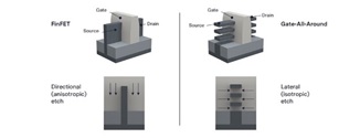
Fig. 1: Transition from finFET
to GAA drives critical isotropic selective etch requirements. Source: Lam Research
Used for several decades, etch is an essential process
in the fab. In a simple process flow, a system deposits silicon dioxide materials
on a wafer. A lithography system then patterns tiny features on the materials for
each die on the wafer, and the etch tool removes unwanted materials on each die
to create various structures with the goal of angstrom-level precision (1Å = 0.1nm).
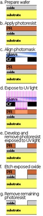
Fig. 2: General patterning and etching process steps
in a fab. Source: Wikipedia
Basically, an advanced etch tool is a standalone system
with a chamber. In operation, a wafer is inserted in the chamber. In one type of
etch, plasma — which is an ionized gas — is generated in the chamber. “First of
all, we make a plasma. Electrons strike gas molecules. That creates ions and more
electrons. They also create free radicals. The radicals become the species that
performs the chemical etching in a plasma etch system. These free radicals diffuse
to the wafer surface. It might react with one material but not another. Finally,
you have an etch. The result is an isotropic process. Given
the right chemistry, it can be very highly selective,” explained Chris Mack, CTO
of Fractilia, in a video presentation. Basically, a free
radical is an atom, molecule or ion.
Not all chip processes require highly-selective etches.
In chip production, many etch steps are straightforward and use existing etch tools.
For more demanding chip processes, etch vendors provide various options involving
more sophisticated tools. Highly-selective etch is one such option. Using proprietary
chemistries, an etch tool with these capabilities removes targeted materials without
modifying or removing the surrounding layers.
This process resembles atomic layer etch (ALE), but they
are different in many respects. Basically, ALE selectively removes targeted materials
at the atomic scale. “In ALE, you are trying to remove one atomic layer at a time.
You have extreme uniformity, and you don’t have to remove the entire film,” said
Dan Hutcheson, vice chairman of TechInsights. “With selective
etch, you are hammering away at the film until it’s all gone. The advantage of selective
etch is that you can go much faster. A key to that is you can’t damage what’s underneath
it or around it.”
Selective etch also involves other factors. “By definition,
as you etch, selectivity is the ratio between what you’re trying to remove and what
you don’t want to remove,” Hutcheson said.
In one example, a chipmaker deposits a silicon dioxide
material on a substrate. The chipmaker wants to keep a select portion of that material
on the middle of the device, but would like to remove the rest. To accomplish that,
a photoresist mask material is deposited on the middle portions.
During the etch process, etchants (plasma, gas/vapor,
acids) in the chamber bombard the wafer. The etching species react slower to the
mask material, but reacts faster with and removes the exposed silicon dioxide.
Selectivity refers to the difference in reactivity between
the exposed material and its underlayer or the exposed
material and neighboring material. Put another way, selectivity is the ratio of
etch rates between any two materials, according to equipment maker Corial, a Plasma-Therm Company.
“Selective etching refers to the process of removing
material with extreme selectivity at >1000:1, and little material loss: <2Å
or one monolayer of atoms. To put that into context, normal etch selectivity is
in the 20:1 range,” said Ian Latchford, director of product marketing at Lam Research.
Nonetheless, highly-selective etches are required for
a growing number of applications. All of these require specialized and expensive
selective etch tools with complex chemistries.
Etch modes
In total, the global etch market grew from $14 billion
in 2020 to $19.9 billion in 2021, according to TechInsights.
The etch market is expected to grow by an annual rate of 7% over the next five years,
according to the firm. AMEC, Applied Materials, Hitachi, Lam, Plasma-Therm and TEL are among the players in the etch business.
In the early days of the IC industry, chipmakers built
their own equipment. In those days, etch processes were conducted in sinks beneath
fumed hoods, according to historical documents from VLSI Research, now part of TechInsights. Basically, wafers were submerged in a sink filled
with chemical etchants and then rinsed. This removed the materials on the wafer.
In the late-1960s, Signetics,
a now-defunct chipmaker, performed the earliest work in plasma etching. By the 1970s,
several commercial etch equipment vendors had emerged.
Early on, etch technology morphed into two segments—wet
etch and dry etch. In a system, wet etch removes materials by submerging wafers
in liquid solutions.
Dry etch, the bigger of the two markets, is widely used
for the production of today’s chips. Dry etching is split into three segments or
modes — plasma etch, reactive ion etching (RIE), and sputter etch (a.k.a., ion beam
etch). Each mode is used for different applications.
Technically, selective etch is an application rather
than a separate category. It fits under both the wet and dry etch categories. In
all cases, the goal is to perform precise etches with good uniformities on the wafer.
Sputter or ion beam etch is a physical process. In operation,
a wafer is inserted in a system. The tool generates ions at accelerated rates, thereby
removing materials in chips.
Developed in the 1970s, RIE is a plasma process, which
is widely used in today’s chips. In operation, ions are generated in a system, which
then bombards the surface of the wafer. This, in turn, removes materials in chips.
Plasma etching, meanwhile, is different. “In this system,
the first step is to create a high-density plasma, which consists of many electrons,
ions and neutrals of different reactivities,” said Philippe
Bézard, an etch R&D engineer at Imec. “Then you filter out the ions with either an ion filter
(visualize a plate with small holes through it) or with a larger gas pressure to
the wafer to let time neutralize the ions.”
The remaining radicals diffuse on top of the wafer surface
and are then absorbed. “A reaction is triggered between the atoms from the substrate
and other molecules from the gas phase to form volatile molecules,” Bézard said.
Each etch mode has different attributes, such as selectivity
and directionality. Directionality involves anisotropic and isotropic etching.
“(In sputter etching), we can get high anisotropy, but
not high selectivity,” explained Fractilia’s Mack. “RIE
can produce good selectivity, high anisotropy, and moderate etch rates. Control
is sometimes difficult.”
At times, chipmakers require more unidirectional and
selective etches. That’s where plasma etch comes in. “Generally, this process is
isotropic with potentially high selectivity,” Mack said. “To get more selectivity,
we need chemistry.”
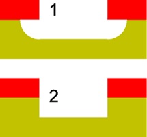
Fig. 3: Isotropic or multidirectional etch (top) vs.
anisotropic or directional etch (bottom) Source: Wikipedia
ALE vs. selective etch
Highly-selective etch is required for many advanced
chips. Over the years, the semiconductor industry has developed new and complex
devices for both memory and logic.
Starting in 2011, some foundry vendors began to offer
advanced processes using state-of-the-art finFET transistors. IC vendors
have developed chips around finFETs. Today, foundry customers
are shipping chips using finFETs at the 16nm/14nm, 7nm
and 5nm process nodes. 3nm finFETs are in R&D.
In addition, at 3nm and/or 2nm, some foundries will
migrate to gate-all-around (GAA), which are faster
transistors that consume less power than finFETs. But
GAA FETs also are more expensive and harder to fabricate.
At the same time, memory makers are developing more
advanced 3D NAND, DRAMs, and various next-generation memory types.
These devices present significant manufacturing challenges
for device makers, which is influencing the development of more advanced processes
and tools. For advanced transistors and the latest DRAMs, chipmakers are using extreme ultraviolet (EUV) lithography,
a 13.5nm wavelength system used to pattern tiny features in chips.
Suppliers of deposition and etch tools also face several
challenges. “There are a lot of process challenges,” said Robert Clark, senior member
of the technical staff at TEL, during a presentation at the recent IEDM conference.
“Every generation leads to higher and higher aspect ratios that we have to deal
with. That creates all kinds of etch problems. You have problems with deposition,
as well. You have conformality, voids and seams in your
depositions. You have bowing, bending, loading, and selectivity problems in etching.”
Fortunately, etch suppliers have developed several new
capabilities to address these challenges. ALE and highly-selective etch are among
the innovations.
After years in R&D, etch suppliers introduced ALE
processes in the mid-2010s. ALE selectively removes targeted materials at the atomic
scale.
In one example of ALE, a wafer resides in a chamber
in an ALE system. The first step is to inject chlorine gas on a silicon surface
in the chamber. The chlorine molecules are absorbed on the surface, which modifies
the surface. Then, argon ions are injected in the chamber, bombarding the surface
and removing the modified layer.
There are two types of ALE—plasma and thermal. Plasma
ALE, which is in production, enables anisotropic etches. Thermal ALE, which is still
taking root, uses thermal reactions for isotropic etches.
“Plasma or thermal ALE are more about extreme control
of the etch front rather than overall selectivity,” Imec’s Bézard said. “Sometimes it’s
better than conventional plasma etching, sometimes it’s
worse. But the selectivity is much below what is required and achieved for highly-selective
etch.”
In addition, ALE is slow and has limited isotropic capabilities.
And in some cases, ALE can cause minimum damage to structures.
Highly-selective etch is different. “Highly-selective
etch can be an etching method on its own. Highly-selective etch is a technology
that enables applications where selectivity is the most important spec,” Imec’s Bézard said.
For years, selective etch has been used in chip production,
but the technology was limited. “Prior to the introduction of the early selective
etch systems, chipmakers who wanted to perform isotropic etching would use wet etch,”
Lam’s Latchford said. “But wet etch is extremely limited in terms of precision,
control, and materials, and is simply not capable of creating the new device structures
chipmakers need to continue evolving to smaller nodes.”
Over time, the industry developed selective etch processes
using dry etch. Today, Applied, Lam, TEL, and others offer tools with next-generation
selective etch capabilities. Vendors use different names for the same process. Some
call it extreme selective etch, highly-selective etch, or precision selective etch.
But all of them use dedicated chambers to achieve highly-selective etching using
proprietary chemistries. The chambers are incorporated on standard etch platforms.
For its selective etch system, Applied uses a two-step
approach to enable isotropic etches. First, the surface is treated. Then, radicals
are generated, thereby removing the targeted materials.
“The radical-based approach gives extremely high selectively.
It can etch one material and not touch another surface,” explained Uday Mitra, a vice president at Applied
Materials, in an interview in 2017.
Lam, meanwhile, recently introduced three selective
etch products—Argos, Prevos and Selis.
Using novel chemistries, Prevos provides selective etches
for oxide, silicon and metal. Selis employs radical and
thermal etch capabilities for selective etching. And Argos selectively modifies
and decontaminates wafer surfaces.
Highly-selective etch can be used in both anisotropic or isotropic applications for memory and logic
devices. Each application also could have different selectivity.
“It all depends on the application and type of etch
used,” Imec’s Bézard said “For
plasma etching, a selectivity of 50:1 between different polymers would be considered
very high. It’s usually <10:1. That would be considered very low when etching
silicon selectivity to oxide using cyclic processes for instance (typically >300:1).”
All processes are challenging, regardless of the application.
“There’s a generic etch, which has a certain selectivity. And then, when you get
to selective etch, you are talking about multiple orders of magnitude of greater
selectivity,” TechInsights’ Hutcheson said. “When you
go to something like a purely selective etch, it’s much closer to a pure chemical
process. But now you have to figure how to make the chemistry work. You want to
over-etch a bit, so that you make sure you clear all the material. But you can’t
go too far or you’re going to start removing the underlying materials. The more
you can increase the selectivity, the more you can make sure you have a uniform
etch across a 300mm wafer. We’re talking about angstroms that we deal with, in terms
of our precision that has to be across a 300mm water. The precision is phenomenal.”
The apps
There are several applications for highly-selective
etch. For example, self-aligned contacts are formed using anisotropic highly-selective
etch. In chips, contacts are tiny structures that connect the transistor with the
first layer of copper interconnects in devices.
Meanwhile, in 2020, TEL and Imec
presented a paper on an isotropic plasma-free process for silicon trimming applications.
Basically, the etch tool trims a film or material in order to form the desired shape
of the structure. This process could be used for finFETs
and GAA.
Other selective etch processes are used in GAA. At the
3nm and/or 2nm process nodes, leading-edge foundries and their customers eventually
will migrate to a GAA transistor type called a nanosheet FET. A nanosheet FET is a finFET that has been rotated by 90 degrees, resulting in horizontally
stacked fins with a vertical gate material in between each fin. Each fin, which
resembles a sheet, is a channel.
To make nanosheets in the
fab, an epitaxial tool deposits ultra-thin, alternating layers of silicon-germanium
(SiGe) and silicon on a substrate, forming a superlattice structure. This structure might have three, five,
or more layers of each material.
Tiny vertical fins are patterned and etched in the superlattice structure. Then, inner spacers are formed. For
this, the outer portions of SiGe layers in the superlattice structure are recessed and then filled with dielectric
material.
“The inner spacer module provides control of the effective
gate length, and also isolates the gate from the source/drain epi,” said Andrew
Cross, process control solutions director at KLA. “At each of these steps in the inner spacer formation,
precise control of the shape and CD of the indents and final spacer recess is critical
to ensure correct device performance.”
Next, the source/drain is formed. Then, the SiGe layers in the superlattice structure
are removed, leaving silicon-based layers or sheets, which make up the channels.
“Channel release requires individual control of sheet
height, corner erosion, and channel bending,” said Scott Hoover, senior director
of strategic programs at Onto Innovation.
Finally, a gate is formed by depositing a high-k dielectric
and metal gate materials. Each step presents some challenges, particularly the inner
spacer and channel release processes.
“For each of these critical steps in nanosheet device fabrication, the key is to employ a highly-selective
gas phase etch process,” said Nicolas Loubet, a senior
technical staff member at IBM Research. “Regarding the channel release, a high >150:1
SiGe versus Si etch selectivity is required to prevent
nanosheet silicon channel loss, which could lead to mobility
degradation, high channel resistance and a large variability across the devices
with different nanosheet widths. The etch process also
needs to completely etch the SiGe in small cavities with
a controlled etch rate and should not become self-limited.”
In a recent paper, IBM and TEL demonstrated a lateral
dry etch technique for GAA using novel chemistries, enabling a >150:1 selectivity.
Lam, meanwhile, also has developed a highly-selective
etch process for the GAA inner spacer and release steps. For the channel recess
step, for example, Lam combines its new Prevos and Selos tools.
“In GAA structures, only the SiGe
material layer is removed, while every other piece of a device is left relatively
untouched. With this capability, chipmakers can sculpt nanoscale features that require
angstrom-level precision to avoid removing, modifying or damaging other critical
material layers during the etch process,” Lam’s Latchford said.
Regardless of the tool vendor, it’s a difficult process.
“The challenge is not so much finding the chemistries,” Imec’s
Bézard said. “It’s also getting the exact same selectivity
for each nanosheet, as the bottom one will see more of
the interaction of the etch gas with the substrate than the top one. So you can
have very local differences. That is where we need magic. We need to ensure every
nanosheet sees the same thing as the others.”
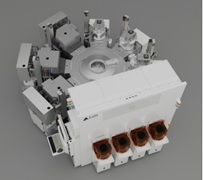
Fig. 4: Lam’s Selis-Prevos
system etches SiGe/Si stacks in nanosheet
FETs and other processes. Source: Lam Research
Future devices
Highly selective etch also is required for future devices
such as complementary FETs (CFETs), a 3D
stacked logic device. CFETs currently are in R&D.
Memory is another application. Today, memory makers
are pushing into the next phase of DRAM scaling, but they are facing several challenges
as the technology approaches its physical limit.
In response, memory makers are working on 3D DRAMs,
which in many respects resemble 3D NAND. 3D DRAMs are several years away from mass
production. “In 3D DRAM, the big design change gets around a lot of the scaling
issues faced in the planar designs, and at the same time, creates a big need for
lateral selective etches,” Lam’s Latchford said.
Conclusion
To be sure, the industry is working on a range of future
devices. Chipmakers require more advanced tools in several segments, such as deposition,
inspection, lithography and metrology.
Highly-selective etch is an important addition to the
mix of tools. “These solutions enable chipmakers to create increasingly powerful
and complex chips that can support compute and performance-intensive technologies,
such as self-driving vehicles, advanced digital healthcare and the forthcoming metaverse,” Latchford said.