Intel, TSMC, Samsung, Arm, Google, Microsoft Form
Consortium to Define Standards for Advanced Chip-Packaging Tech as Moore's Law
Slows Down
Intel, TSMC, Samsung, AMD, Arm, Advanced Semiconductor Engineering,
Google Cloud, Intel, Meta (Facebook™s parent
company), Microsoft, Qualcomm recently announced the creation of a new
Universal Chiplet Interconnect Express (UCIe) standard for better chiplet
interoperability.
The new UCIe consortium aims to
standardise die-to-die interconnection between chiplets, which are blocks of interconnected circuits found
in modern chips. (An individual chip is called a die before it is packaged).
This will enable end users to mix- match chiplet
components and build customized systems-on-a-chip (SoC)
using parts from different vendors.
So what is the driving force behind the world's three
biggest chipmakers, along with several other leading tech companies deciding to
form a consortium and collaborate?
To understand the context, let us start with what may be
a more familiar term - the motherboard found inside, say a personal computer.
The motherboard is the central board that hosts and
connects together various detachable and replaceable child components including
integrated circuits commonly known as chips. Each of these chips may serve a
variety of purposes, for example, the central processing unit (CPU), Graphical
Processing Unit (GPU), primary or secondary memory units, signal processing
related RF/Analog/mixed-signal chips, input/output interfaces, and so on.
In contrast, a SoC integrates
most or all of these into a single 'unit'. SoCs are
typically used for mobile computing (smartphones, tablets etc),
embedded systems and in applications where previously microcontrollers would be
used.
Samsung's Exynos used in its
Galaxy series of smartphones, Qualcomm's Snapdragon used in smartphones of
various brands as well as Apple's M1 used in its Macintosh desktops are good
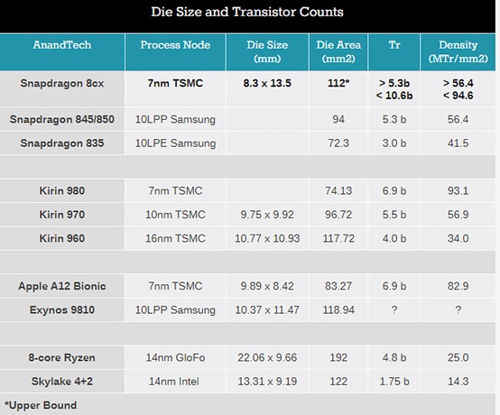
examples. Below is a table that shows some more examples.
Die Size
There were however some challenges in future roadmaps in
making the SoCs as a single chip - i.e as a monolithic IC.
1) The die sizes are now agetting
closer to the approximately 26mm X 32 mm limit of lithography tools - for example,
Apple M1 Max die size is reportedly 20mm X 22mm
2) Not all elements of an SoC need to be manufactured using the most advanced process
node. Analog chips for example need mature node processes.
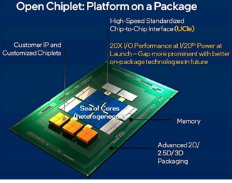
Open Chiplet
Combined, a new concept of "chiplet
based SoCs" is gaining popularity driven by an
enabling technology broadly known as heterogeneous integration or multi chip
module (MCM) packaging.
As this piece in Next
Platform notes, every compute
and networking chip vendor is looking at 2D, 2.5D, and 3D chiplet
architectures as they snap their chips into pieces to make them more manufacturable at an economic cost as Moore’s
Law slows down.
A white paper titled
'Chiplets - Taking SoC
Design Where no Monolithic IC has Gone Before' (published in April 2019) noted that in the earlier days
of MCM design, engineers used ad hoc approaches for die-to-die interconnect.
"The connections between and among die in an MCM
conformed to no industry standards, because such standards did not exist (and
still do not). For chiplet-based design to take off,
ad hoc connections cannot be the norm. Standards are needed just as they were
for computer peripherals (RS-232, GPIB, SCSI, PCIe,
etc.) and for networking (Ethernet)." the paper observed.
That standardisation is what
the UCIe consortium hopes to achieve.
"Taking significant inspiration from the very
successful PCI-Express playbook, with UCIe the
involved firms are creating a standard for connecting chiplets,
with the goal of having a single set of standards that not only simplify the
process for all involved, but lead the way towards full interoperability
between chiplets from different manufacturers,
allowing chips to mix-and-match chiplets as chip
makers see fit." a post in Anandtech wrote summarising the
standardization move.
It further states that "The
specification covers the physical layer, laying out the electrical signaling
standards that chiplets will use to talk to each
other, as well as the number of physical lanes and the supported bump pitches.
And the specification covers the protocol layer, defining the higher-level
protocols overlaid on those signals to make sense of everything and to provide
the necessary feature set" (Note: bumps refer to solder bumps
that are done at the end of IC fabrication and pitch is the distance between 2
bumps)
Also note that "What
the specification doesn’t cover, however, is the
packaging/bridging technology used to provide the physical link between chiplets. UCIe is
bridge-agnostic; chiplets can be linked via fanout bridge,
silicon interposers, EMIB, or even just a plain old organic substrate in the
case of lower bandwidth devices"
In a scenario where packaging techniques are becoming
more and more important to sustain scaling and performance advancements, key
players coming together as a consortium to agree upon standards is surely
encouraging.