Transistors Reach
Tipping Point at 3nm
[ABS News Service/01.03.2022]
The semiconductor industry is making its first major change in a new
transistor type in more than a decade, moving toward a next-generation
structure called gate-all-around (GAA) FETs.
Although GAA transistors have yet to ship, many industry experts are
wondering how long this technology will deliver — and what new architecture
will take over from there. Barring major delays, today’s GAA structures should
perform and extend for three technology nodes of products before they run out
of steam, according to various roadmaps.
Beyond that, the industry is evaluating several transistor candidates,
but each has technical gaps. It will take vast resources and innovations to
develop even one candidate to successfully extend CMOS FETs for another decade.
Near-term, though, the industry has a clear migration path to the
highest performing chips. Traditionally, to advance a new chip, IC vendors
develop a system-on-a-chip (SoC) and then cram more
transistors on the device at each generation. Transistors, a key building block
in chips, act like switches in devices.
This formula, called chip scaling, works as long as the industry can
develop new and faster transistors that consume the same or lower power at
roughly the same cost per chip. Since 2011, vendors have been shipping chips
based on one advanced transistor type—finFETs.
However, finFETs will soon approach its limits,
prompting the need for a new technology at the 3nm and/or 2nm process nodes. (A
node refers to a technology generation’s performance specifications, process
technology and design rules. A process technology is the recipe used to
manufacture a chip in a fab. The chip industry is beginning to refer to nodes
beyond 2nm as the Angstrom nodes.)
At 2nm and/or 3nm, leading-edge foundries and their customers eventually
will migrate to a GAA transistor type called the nanosheet
FET. GAA FETs provides greater performance at lower power than finFETs, but they are more expensive to design and
fabricate.
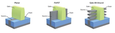
Fig. 1: Planar transistors vs. finFETs vs.
gate-all-around. Source: Lam Research
Engineers know that even today’s GAA designs eventually will run into
performance limitations. The industry is planning ahead by evaluating several
futuristic transistor types beyond 2nm, including 2D devices, carbon nanotube
FETs, CFETs, forksheet FETs and vertical-transport
FETs. So far, there is little consensus beyond 2nm.
While these novel structures can deliver amazing electrical properties,
they are difficult to fabricate. As a result, most will never move from lab to
fab. Realistically, the industry can only afford to back one transistor
candidate.
That’s not the only consideration. “(We have) new transistor
architectures,” said Chung-Hsun Lin, senior director
and principal engineer at Intel, during a presentation at the recent IEDM
conference. “In addition to the technology from the transistor side, there is
already new architectures that are involved, such as new power deliver systems.
And also, there is packaging, which has been popular and important.”
In fact, chiplets, one
form of advanced packaging, are
creating a buzz for several reasons. With chiplets,
the die design is broken up into smaller dies, and once fabricated and singulated, they are re-aggregated into an advanced
package. The chiplet approach accelerates
time-to-market, improves yield, and potentially lowers cost. As pitch scaling
becomes harder and more expensive, stacked chiplet
designs become a compelling solution for specific high-performance
applications.
All told, a holistic approach that optimizes performance from
transistor-to-system is becoming necessary to maintain the industry’s
performance pace.

Fig. 2: Logic Scaling Roadmap from nm to Å. regime Source: Imec
Transistor troubles
For decades, the IC industry followed the same basic formula. Every 18
to 24 months, chipmakers introduced a new process technology with greater
transistor density, thereby lowering the cost per transistor. At each node,
chipmakers scaled the transistor specs by 0.7X, enabling the industry to
deliver a 40% performance boost for the same amount of power and a 50% reduction
in area. Chip scaling fuels most of our new electronic products, which perform
an increasing number of functions at higher speeds using less energy.
Using planar transistors, the semiconductor industry marched down
various process nodes using advancing lithography tools and other process
enhancements at each technology node. Then the industry hit a roadblock at the
20nm technology, around 2011, when planar transistors suffered from
short-channel effects. “For example, current could leak between the source and
drain even when flow should have been turned off,” said Nerissa Draeger, director of university engagements at Lam Research.
Planar transistors are still
optimized for chips at 22nm and above, but the industry required a new solution
going forward. Intel began making finFET transistors
in 2011 at the 22nm node. Foundries moved to finFETs
later, at 16nm/14nm.
FinFETs have several advantages over planar transistors.
“As compared to prior planar transistors, the fin, contacted on three sides by
the gate, provides much better control of the channel formed within the fin,” Draeger said.
Using various process steps in a fab, chipmakers have scaled and
extended finFETs down to 7nm and 5nm, enabling new
and high-performance chips.
However, many chips do not require finFETs.
Digital chips, as well as analog, RF and other devices still utilize planar
transistors. They are all thriving. For example, the 28nm planar products still
constitute one of the largest markets by node.
UMC, for one, saw a 75% revenue jump for its 28nm technology in its most
recent quarter. “The 75% year-over-year revenue increase reflected robust chip
demand related to 5G, IoT, and automotive,” said
Jason Wang, UMC’s
co-president.
On the leading edge, meanwhile, chip scaling faces particular
challenges. At 7nm and below, static leakage has become problematic, and the
power and performance benefits have started to diminish. Currently, performance
increases are in the 15% to 20% range.
When the fin width for finFETs reaches 5nm
(around the 3nm node), the contacted poly pitch (CPP) reaches a limit of
roughly 45nm with a metal pitch of 22nm. CPP is the distance separating the
centers of adjacent gate contacts.
Nonetheless, the industry wants faster chips beyond 5nm. “We could use
10X more computing power even right now,” said Aki Fujimura, CEO of D2S. “Heavy simulation like weather forecasting, bitcoin mining, or deep
learning are driving demand for 3nm and beyond. And fortunately, we will
continue to scale, even though Moore’s Law is changing.”
Coming up: GAA FETs, chiplets
Today, Intel, Samsung and TSMC are developing 3nm processes, and several
companies are developing chips using the technology.
It’s an expensive endeavor. “The average cost of designing a 28nm chip is
$40 million,” said Handel Jones, CEO of IBS. “By comparison, the cost of
designing a 7nm chip is $217 million, and the cost of designing a 5nm device is
$416 million. A 3nm design will cost up to $590 million.”
Plus, foundry customers are facing difficult choices at 3nm. Unlike
previous nodes, where chipmakers followed the same transistor path, foundry
vendors are developing different technologies at 3nm. Samsung plans to migrate
from finFETs at the 5nm node to GAA at the 3nm node.
In contrast, Intel and TSMC plan to extend finFETs at
3nm and then move to GAA at 2nm.
Samsung and TSMC have announced intentions to ramp up their 3nm
processes in the second half of 2022, which is slightly later than expected.
“Both companies have had some delays on 3nm,” said Samuel Wang, an analyst at
Gartner. “The 3nm ramp will take longer than the previous node.”
Nonetheless, each company has a different philosophy. For example, by
extending finFETs to 3nm, TSMC says that its
customers can develop 3nm designs without having to migrate to a new transistor
type, thereby reducing risk.
TSMC’s 5nm and 3nm processes are both based on finFETs,
but they are different. TSMC’s 3nm is a fully scaled version of its 5nm
platform but with greater complexity.
In contrast, Samsung wants to get a jump on the competition in the GAA
era. The company announced that it will introduce an early version of 3nm GAA
in 2022, while its “performance version” will ship in 2023.
That would put Samsung ahead of the competition. “TSMC will most likely
have its 2nm based on GAA, which is targeted for production in 2025. Intel’s
20A process, which is 2nm, is GAA. It is planned to launch in 2024,” Wang said.
All leading chip manufacturers are developing one popular type of GAA
transistor — the nanosheet FET (Intel
calls it a RibbonFET.) A nanosheet
FET is a finFET that has been rotated by 90 degrees,
resulting in horizontally stacked fins with a vertical gate material in between
each fin. Each fin, which resembles a sheet, is a channel.
On the surface, the scaling benefits between 3nm finFETs
and nanosheets appear to be minimal. Based on analyst
estimates, both offer 48nm CPP with a 22nm metal pitch.
Still, nanosheets structures provide
significant advantages. “Gate-all-around, or GAA transistors, are a modified
transistor structure where the gate contacts the channel from all sides and
enables continued scaling,” Lam’s Draeger explained.
“This provides improved channel control relative to finFETs.”
In comparison, with finFETs, the width of the
device is quantized. In nanosheets, designers can
vary the sheet width. A wider sheet provides more drive current and
performance. A narrower nanosheet has less drive
current, but occupies a smaller area.
One drawback with nanosheets is lackluster pFET performance due to low hole
mobility in a silicon-based channel.
IBM described one solution to this problem at IEDM, with a pFET that uses a compressively strained silicon-germanium (SiGe) channel material. “A nanosheet
pFET SiGe channel provides
a 40% mobility increase and a 10% performance gain over a silicon channel, with
reduced threshold voltage (Vt) and improved negative
bias temperature instability (NBTI),” said Ruqiang Bao, senior engineering manager at IBM.
Fabricating nanosheet FETs poses significant
challenges. In the flow, an epitaxial tool deposits ultrathin, alternating
layers of SiGe and silicon on a substrate, forming a
super-lattice structure. This structure might have three, five or more layers
of each material.
Tiny vertical fins are patterned and etched in the super-lattice
structure. Then, inner spacers are formed. In a spacer etch, the outer portions
of SiGe layers in the super-lattice structure are
recessed and then filled with dielectric material.
Next, the source/drain is formed. Then, the SiGe
layers in the super-lattice structure are removed, leaving silicon-based layers
or sheets, which make up the channels. Finally, a gate is formed by depositing
a high-k dielectric and metal gate materials.
Each step is a challenge. As with all processes, the goal is to develop
chips without defects. This requires a sound process control strategy in the
fab.
“The process control challenges are greater in the smaller nodes,” said
Julie Ply, director of quality materials at Brewer Science. “There
are several reason here: 1) detection limits must constantly be reduced to
detect meaningful signals in the smaller nodes; 2) process signals may need to
be further refined and reduced to provide a greater level of control; and 3)
the value of the smaller node materials typically increases, making early
detection and correction more important than ever to mitigate potential
losses.”
At 3nm and beyond, the industry will need new innovations and fab
equipment. Among them are:
o
Extreme ultraviolet (EUV)
lithography. Using a 13.5nm wavelength, EUV has been used to pattern tiny
features at 7nm and 5nm. High-NA EUV, a next-generation version, is in R&D
and needed to pattern finer features beyond 3nm.
o
Atomic-level processing. Atomic layer
deposition (ALD) as well as next-generation etch technologies are required to
deposit and etch materials in structures.
o
Inspection and metrology. New methods are needed to
look for defects and measure them.
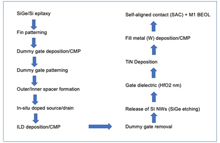
Fig. 3: Process flow for stacked nanosheet
FETs. Source: Leti/Semiconductor Engineering
Transistor fabrication is only part of the 3nm system solution. Chip
design is paramount. On-chip interconnects, assembly and packaging must
minimally impact device and system performance.
There are proven strategies for boosting the bandwidth in systems. For
example, in many systems, a processor, DRAM, and other devices are placed on a
board. Data moves continuously between processor and memory, but at times this
exchange causes latency and increased power consumption. Advanced packaging
allows the placement of memory and processors closer together, enabling
increased bandwidth.
Meanwhile, with chiplets, the design utilizes
smaller dies and/or IP blocks and is developed from the ground up. Then,
packaging houses or IDMs re-aggregate the pieces and assemble them in a
package. Rather than an SoC,
chiplet-based designs are essentially a system in
package. AMD, Intel and Marvell have shipped products based on chiplets.
Still, such heterogenous integration requires
sizable resources. In chiplet-based designs, the dies
are connected using a bus with an interface on each chip. Today’s designs use
proprietary buses and interfaces, but there is a move to develop open buses and
interfaces.
“In all these schemes, data is passed through an interface circuit that
controls the data flow. This includes the addition of control signals,
serializing and deserializing of data, data
conditioning and data error correction. These interface circuits inevitably add
latency to the signals,” said Eric Beyne, senior
fellow and vice president of R&D at Imec.
At IEDM, Imec proposed a solution to the
problem — 3D SoCs. In one example, Imec devised an 3D design with 256
cores. But advanced design capability is necessary. “This requires dedicated
EDA tools that can handle both designs simultaneously, using automated tools
for system partitioning and 3D critical path optimization during
place-and-route, which takes chiplets to the next
level,” said Dragomir Milojevic,
a principal scientist at Imec.
Future options
Chiplet technology continues to evolve, while transistor
scaling slows. Barring any delays, nanosheet FETs are
projected to perform well over three technology generations, from the 3nm node
in 2022, to 2nm in 2025, and to 1.5nm in 2028, according to the International
Roadmap for Devices and Systems (IRDS).
In a paper at IEDM, TEL outlined one possible scaling path for nanosheets. A first-generation nanosheet
FET could consist of three nanosheets, each of which
are 30nm wide, according to TEL. The device features a 48nm CPP and 22nm metal
pitch.
Then, by scaling the device at 0.73X, a second-generation 4-sheet FET
could consist of a =>46nm CPP with a =>18nm metal pitch, the company
said. A third-generation device may scale these dimensions by 0.78X.
By 2031, nanosheet FETs may no longer deliver
expected performance at low power and cost, according to the IRDS. The roadmap
projects a move to a new transistor — complementary FETs (CFETs)
around the 1nm node.
Imec’s roadmap tells a slightly different story. The
research institute projects nanosheet extensions to
2027, followed by the introduction of forksheet FETs. Then,
CFETs would appear around 2029.
Through design and process optimizations, nanosheets
may be extended longer than expected, pushing out the need for forksheets, CFETs, or another candidate. Indeed, the nanosheet FET might be the last transistor type.
Nonetheless, forksheets and CFETs demonstrate
great potential. Both technologies are different from existing GAA, which use
different devices for the nFETs and pFETs.
Imec researchers are the innovators behind forksheet FETs, which feature two nanosheet
FETs next to each other on one device. One nanosheet
FET (three sheets) consists of pFETs, while the other
nanosheet (three sheets) consists of nFETs. A dielectric wall isolates the nFETs
from pFETs.
“You can scale the n-to-p space between the NMOS device and the PMOS
device in the standard cell to create more active device width,” said Sri Samavedam, senior vice president of CMOS technologies at Imec. “It gives you more active width in the same footprint
compared to the nanosheet, and it also has lower
parasitic capacitance, which results in about a 10% performance benefit over nanosheets.”
In the fab, forksheets are manufactured much
like nanosheets, with one big difference. Two nanosheet FETs are fabricated next to each other. Then, a
silicon nitride (SiN) material is deposited between
the two structures, forming the isolation region.
CFETs are like a 3D stacked logic device. In CFETs, you might have six nanosheets, which are vertically stacked on the same
device. The top three nanosheet FETs are pFETs, while the bottom three are nFETs.
“By stacking opposite tone devices vertically rather than placing them
laterally, CFETs eliminate this scaling barrier and are seen as a strong
contender to succeed nanosheets,” said Lars Liebmann, a senior technologist at TEL, in a paper at IEDM.
Recently, Intel presented a paper on a CFET with 13nm wide sheets and
9nm spacing between each one. “The approach combines excellent electrostatics
with a path to significant cell size reduction,” said C.Y. Huang of Intel.
There are two different process flows for CFETs, monolithic and
sequential. Both are complex, and not all of the processes and tools are
commercially available today. It would take an enormous amount of funding to
develop them.
The monolithic approach involves a CMOS flow with more complexity. “The
monolithic CFET approach refers to building both the NMOS and PMOS device on
the same wafer,” Imec’s Samavedam
said. “The active areas and gates of both devices are self-aligned. The flow
requires several high-aspect ratio processing steps like depositions and
etches. That needs to be developed.”
In the sequential approach, NMOS and PMOS transistors are processed on
separate wafers, which are then bonded. “With the sequential CFET approach, the
NMOS and PMOS devices can be formed on separate wafers so that they can be
individually optimized like having different channel materials or substrate
orientation,” Samavedam said. “The challenge is that
the active areas and gates are not self-aligned. It requires high accuracy top
and bottom wafer alignment and bonding, as well as novel integration to connect
the top and bottom device gates. The sequential CFET will also require more
processing steps since each device is built separately.”
Distant future options
For years, the industry has been working on 2D-material FETs. Still in
R&D, these devices could appear after 2030, providing they achieve
commercial viability.
2D FETs resemble nanosheet FETs. The big
difference is the channel is based on a transition-metal-dichalcogenide
(TMD) material, such as molybdenum disulfide (MoS2), tungsten
selenite (WSe2) and others materials. TMDs enable thinner channels
for gate-length scaling as well as high channel mobilities..
At IEDM, Intel described various 2D FETs including a nanoribbon FET with
5nm gate length. In another example, Intel described a PMOS device using a WSe2
film to achieve a 141mV/dec sub-threshold swing.
Imec’s Samavedam spoke to
challenges with 2D FETs. “There are still many fundamental materials issues
that need to be resolved with these materials, like reducing defectivity, variability, improving the channel mobility,
forming low-resistance contacts, doping, and forming scaled gate dielectrics.”
Other technologies are also in R&D, including carbon nanotube FETs.
In these devices, tiny nanotubes make up the channels. Meanwhile, IBM and
Samsung recently described vertical FETs, in which the gate wraps around a
vertically aligned source and drain. The companies said that because there is
no lateral flow of transistor current in this FET, transistor density and
performance substantially improved.
Conclusion
The advanced transistor structures including nanosheet
FETs, 2D-FETs and other structures, are intriguing. Beyond today’s GAA FETs
which have yet to ship, CFETs appear to be gaining momentum, but that could
change.
It’s safe to say that while most of the R&D architectures will not
be commercially implemented, now is the time to develop and select the
structure most qualified for use in 10 years. The best transistor is not just
the one that delivers ultimate device performance. It also must prove to be
production-worthy and cost-effective.